555 Timer Schematic Diagram : Arduino Lesson 555 Timer Ic Osoyoo Com : Jul 24, 2019 · the working principle of the 555 timer is by considering the block diagram of the 555 timer ic.
byAdmin•
0
555 Timer Schematic Diagram : Arduino Lesson 555 Timer Ic Osoyoo Com : Jul 24, 2019 · the working principle of the 555 timer is by considering the block diagram of the 555 timer ic.. Working and schematic diagram of clap swith circuit You can explore various applications based on monostable multivibrator in 555 timer circuits. The threshold input (pin 6) is connected to ground to ensure that it cannot reset the bistable circuit as it would in a normal timing application. The reset input current draw illustrates the need for a current limiting resistor as shown in some of the preceding circuits. You can watch how each of the circuits in this tutorial work in this video:
You can explore various applications based on monostable multivibrator in 555 timer circuits. The control input is used in some of the applications, but most of the applications the control input is not used hence the control voltage is equal to +2/3 vcc. You can watch how each of the circuits in this tutorial work in this video: The 555 timer is a chip that can be us… Sep 29, 2015 · you can also calculate the t with this 555 timer monostable calculator.
555 Timer Ic Introduction Basics Working With Different Operating Modes from www.engineersgarage.com The book has lots of information about the 555 timer, opamps, and other ic's too. 1 by forrest mims is a great resource to have on your bench. Then the bistable 555 timer is stable in both states, "high" and "low". The 555 timer is a chip that can be us… The first comparator has threshold input to pin 6 and control inputs for pin 5. You can explore various applications based on monostable multivibrator in 555 timer circuits. Above schematic diagram shows the 555 timer monostable multivibrator circuit. Sep 29, 2015 · you can also calculate the t with this 555 timer monostable calculator.
Jun 03, 2021 · if you want to learn more about the 555 timer, the book timer, op amp, and optoelectronic circuits and projects book vol.
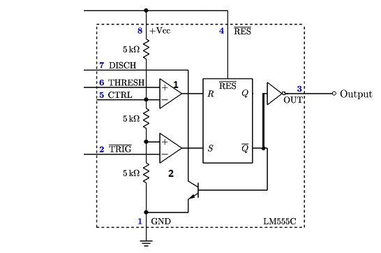
555 ic timer block diagram 555 ic timer block diagram. When the normal high trigger input value instantaneously reduce then the 1/3 v cc, then the output of comparator b becomes high from low, as a result, rs latch or rs flip flop goes to "set". This tutorial provides sample circuits to set up a 555 timer in monostable, astable, and bistable modes as well as an in depth discussion of how the 555 timer works and how to choose components to use with it. The next diagram shows the basic current consumption of 555 timer chips from different manufacturers. Above schematic diagram shows the 555 timer monostable multivibrator circuit. The book has lots of information about the 555 timer, opamps, and other ic's too. 555 timer helpers schematic the addition of a capacitor to the trigger will not work for short output pulses as there is also a short delay in the recovery of the trigger terminal voltage. When flip flop goes to set, then output (at point 3) becomes high. 1 by forrest mims is a great resource to have on your bench. Working and schematic diagram of clap swith circuit The 555 timer is a chip that can be us… You can watch how each of the circuits in this tutorial work in this video: Jun 03, 2021 · if you want to learn more about the 555 timer, the book timer, op amp, and optoelectronic circuits and projects book vol.
555 timer internal schematic diagram. The first comparator has threshold input to pin 6 and control inputs for pin 5. The second 555 timer helper will extend the timers output duration without having to use large values of r1 and/or c1. The book has lots of information about the 555 timer, opamps, and other ic's too. You can watch how each of the circuits in this tutorial work in this video:
Use A 555 Timer As A Switch Mode Power Supply Edn from www.edn.com This 555 timer circuit will remain in either state indefinitely and is therefore bistable. The threshold input (pin 6) is connected to ground to ensure that it cannot reset the bistable circuit as it would in a normal timing application. Above schematic diagram shows the 555 timer monostable multivibrator circuit. Then the bistable 555 timer is stable in both states, "high" and "low". The 555 timer is a chip that can be us… The reset input current draw illustrates the need for a current limiting resistor as shown in some of the preceding circuits. The second 555 timer helper will extend the timers output duration without having to use large values of r1 and/or c1. You can watch how each of the circuits in this tutorial work in this video:
Sep 29, 2015 · you can also calculate the t with this 555 timer monostable calculator.
The next diagram shows the basic current consumption of 555 timer chips from different manufacturers. The block diagram of a 555 timer is shown in the above figure. Working and schematic diagram of clap swith circuit Resistive network consists of three equal resistors and acts as a voltage divider. This 555 timer circuit will remain in either state indefinitely and is therefore bistable. Above schematic diagram shows the 555 timer monostable multivibrator circuit. 555 ic timer block diagram 555 ic timer block diagram. The second 555 timer helper will extend the timers output duration without having to use large values of r1 and/or c1. This tutorial provides sample circuits to set up a 555 timer in monostable, astable, and bistable modes as well as an in depth discussion of how the 555 timer works and how to choose components to use with it. Sep 29, 2015 · you can also calculate the t with this 555 timer monostable calculator. When the normal high trigger input value instantaneously reduce then the 1/3 v cc, then the output of comparator b becomes high from low, as a result, rs latch or rs flip flop goes to "set". Some devices will not function properly if the current to the threshold input is not restricted. The first comparator has threshold input to pin 6 and control inputs for pin 5.
You can watch how each of the circuits in this tutorial work in this video: 555 timer internal schematic diagram. This tutorial provides sample circuits to set up a 555 timer in monostable, astable, and bistable modes as well as an in depth discussion of how the 555 timer works and how to choose components to use with it. Some devices will not function properly if the current to the threshold input is not restricted. When the normal high trigger input value instantaneously reduce then the 1/3 v cc, then the output of comparator b becomes high from low, as a result, rs latch or rs flip flop goes to "set".
The General 555 Timer Circuit Schematic At The Heart Of The Circuit Is Download Scientific Diagram from www.researchgate.net This tutorial provides sample circuits to set up a 555 timer in monostable, astable, and bistable modes as well as an in depth discussion of how the 555 timer works and how to choose components to use with it. Jun 03, 2021 · if you want to learn more about the 555 timer, the book timer, op amp, and optoelectronic circuits and projects book vol. Then the bistable 555 timer is stable in both states, "high" and "low". The next diagram shows the basic current consumption of 555 timer chips from different manufacturers. 555 ic timer block diagram 555 ic timer block diagram. 1 by forrest mims is a great resource to have on your bench. Working and schematic diagram of clap swith circuit When the normal high trigger input value instantaneously reduce then the 1/3 v cc, then the output of comparator b becomes high from low, as a result, rs latch or rs flip flop goes to "set".
This 555 timer circuit will remain in either state indefinitely and is therefore bistable.
The second 555 timer helper will extend the timers output duration without having to use large values of r1 and/or c1. This tutorial provides sample circuits to set up a 555 timer in monostable, astable, and bistable modes as well as an in depth discussion of how the 555 timer works and how to choose components to use with it. Some devices will not function properly if the current to the threshold input is not restricted. 1 by forrest mims is a great resource to have on your bench. You can explore various applications based on monostable multivibrator in 555 timer circuits. The threshold input (pin 6) is connected to ground to ensure that it cannot reset the bistable circuit as it would in a normal timing application. Above schematic diagram shows the 555 timer monostable multivibrator circuit. The control input is used in some of the applications, but most of the applications the control input is not used hence the control voltage is equal to +2/3 vcc. 555 timer helpers schematic the addition of a capacitor to the trigger will not work for short output pulses as there is also a short delay in the recovery of the trigger terminal voltage. The next diagram shows the basic current consumption of 555 timer chips from different manufacturers. The block diagram of a 555 timer is shown in the above figure. Then the bistable 555 timer is stable in both states, "high" and "low". 555 timer internal schematic diagram.